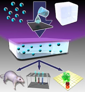
LEDs based on solution-processed inorganic nanocrystals have promise for use in environmental and biomedical diagnostics, because they are cheap to produce, robust, and chemically stable. But development has been hampered by the difficulty of achieving ultraviolet emission. In their paper, Los Alamos National Laboratory's Sergio Brovelli in collaboration with the research team lead by Alberto Paleari at the University of Milano-Bicocca in Italy describe a fabrication process that overcomes this problem and opens the way for integration in a variety of applications.
The world needs light-emitting devices that can be applied in biomedical diagnostics and medicine, Brovelli said, either as active lab-on-chip diagnostic platforms or as light sources that can be implanted into the body to trigger some photochemical reactions. Such devices could, for example, selectively activate light-sensitive drugs for better medical treatment or probe for the presence of fluorescent markers in medical diagnostics. These materials would need to be fabricated cheaply, on a large scale, and integrated into existing technology.
The paper describes a new glass-based material, able to emit light in the ultraviolet spectrum, and be integrated onto silicon chips that are the principal components of current electronic technologies.

Caption: Embedding nanocrystals in glass provides a way to create UV-producing LEDs for biomedical applications.
Credit: Los Alamos National Laboratory. Usage Restrictions: None.The new devices are inorganic and combine the chemical inertness and mechanical stability of glass with the property of electric conductivity and electroluminescence (i.e. the ability of a material to emit light in response to the passage of an electric current).
As a result, they can be used in harsh environments, such as for immersion into physiologic solutions, or by implantation directly into the body. This was made possible by designing a new synthesis strategy that allows fabrication of all inorganic LEDs via a wet-chemistry approach, i.e. a series of simple chemical reactions in a beaker. Importantly, this approach is scalable to industrial quantities with a very low start-up cost. Finally, they emit in the ultraviolet region thanks to careful design of the nanocrystals embedded in the glass.
In traditional light-emitting diodes, light emission occurs at the sharp interface between two semiconductors. The oxide-in-oxide design used here is different, as it allows production of a material that behaves as an ensemble of semiconductor junctions distributed in the glass.
This new concept is based on a collection of the most advanced strategies in nanocrystal science, combining the advantages of nanometric materials consisting of more than one component. In this case the active part of the device consists of tin dioxide nanocrystals covered with a shell of tin monoxide embedded in standard glass: by tuning the shell thickness is it possible to control the electrical response of the whole material.
###
The paper was produced with the financial support of Cariplo Foundation, Italy, under Project 20060656, the Russian Federation under grant 11.G34.31.0027, the Silvio Tronchetti Provera Foundation, and Los Alamos National Laboratory's Directed Research and Development Program.
The paper is titled, "Fully inorganic oxide-in-oxide ultraviolet nanocrystal light emitting devices," and can be downloaded from the following online Nature Communications link: dx.doi.org/10.1038/ncomms1683
Its authors are Sergio Brovelli1, 2, Norberto Chiodini1, Roberto Lorenzi1, Alessandro Lauria1, Marco Romagnoli3,4& Alberto Paleari1
1. Department of Materials Science, University of Milano-Bicocca, Italy.
2. Chemistry Division, Los Alamos National Laboratory, Los Alamos, New Mexico.
3. Material Processing Center, Massachusetts Institute of Technology, Cambridge, Massachusetts..
4. On leave from Photonic Corp, Culver City, California.
Contact: Nancy Ambrosiano nwa@lanl.gov 505-667-0471 DOE/Los Alamos National Laboratory
