Spectrometers have conventionally been expensive and bulky bench-top instruments used to detect and identify the molecules inside a sample by shining light on it and measuring different wavelengths of the emitted or absorbed light. Previous efforts toward miniaturizing spectrometers have reduced their size and cost, but these reductions have typically resulted in lower-resolution instruments.
"For spectrometers, it is better to be small and cheap than big and bulky -- provided that the optical performance targets are met," said Ali Adibi, a professor in the School of Electrical and Computer Engineering at the Georgia Institute of Technology. "We were able to achieve high resolution and wide bandwidth with a compact single-mode on-chip spectrometer through the use of an array of microdonut resonators, each with an outer radius of two microns."
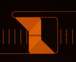
The 81-channel on-chip spectrometer designed by Georgia Tech engineers achieved 0.6-nanometer resolution over a spectral range of more than 50 nanometers with a footprint less than one square millimeter. The simple instrument -- with its ultra-small footprint -- can be integrated with other devices, including sensors, optoelectronics, microelectronics and microfluidic channels for use in biological, chemical, medical and pharmaceutical applications.

Caption: This is a micrograph of the microspectrometer developed Ali Adibi, a professor in the School of Electrical and Computer Engineering at Georgia Tech. The intstrument achieved 0.6-nanometer resolution over a spectral range of more than 50 nanometers with a footprint less than one square millimeter.
Credit: Georgia Tech/Zhixuan Xia. Usage Restrictions: None.

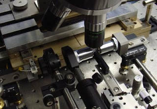
Caption: Experimental setup used to test the 81-channel on-chip microspectrometer designed by Georgia Tech engineers led by Ali Adibi, a professor in the School of Electrical and Computer Engineering.
Credit: Georgia Tech/Zhixuan Xia. Usage Restrictions: None.The microspectrometer architecture was described in a paper published on June 20 in the journal Optics Express. The research was supported by the Air Force Office of Scientific Research and the Defense Advanced Research Projects Agency.
"This architecture is promising because the quality-factor of the microdonut resonators is higher than that of microrings of the same size," said Richard Soref, a research scientist in the U.S. Air Force Research Laboratory at Hanscom Air Force Base who was not directly involved in the research. "Having such small resonators is also an advantage because they can be densely packed on a chip, enabling a large spectrum to be sampled."
Adibi's group is currently developing the next generation of these spectrometers, which are being designed to contain up to 1000 resonators and achieve 0.15-nanomater resolution with a spectral range of 150 nanometers and footprint of 200 micrometers squared.
Adibi, current graduate student Zhixuan Xia and research engineer Ali A. Eftekhar, and former research engineers Babak Momeni and Siva Yegnanarayanan designed and implemented the microspectrometer using CMOS-compatible fabrication processes. The key building element they used to construct the device was an array of miniaturized microdonut resonators, which were essentially microdiscs perforated in their centers. This research built on former Georgia Tech graduate student Mohammad Soltani's work to develop miniature microresonators, which was published in the Sept. 13, 2010 issue of the journal Optics Express.
The researchers adjusted the resonance wavelengths of different microdonut resonators by engineering their geometry. While the resonance was very sensitive to variations in the outer radius, fine-tuning could be achieved by adjusting the inner radius.
The microdonut resonators were carefully designed so that each of the resonators only tapped a small portion of the incoming spectrum, thus enabling measurement of the entire spectrum of desired wavelengths in real time.
A key advantage of this microspectrometer design, according to the researchers, is the ability to independently control and configure the resolution and operating bandwidth of each channel for different applications. The device can cover a wide range of wavelengths from approximately one to three micrometers. Extending this concept to the silicon nitride platform also enables spectrometers for visible light applications.
"The microspectrometer we designed may allow individuals to replace the big, bulky, high- resolution spectrometers with a large bandwidth they are currently using with an on-chip spectrometer the size of a penny," noted Adibi. "Our device has the potential to be a high-resolution, lightweight, compact, high-speed and versatile microspectrometer with a large dynamic range that can be used for many applications."
###
Current graduate students Qing Li and Maysamreza Chamanzar also contributed to this work.
This research was supported by the Defense Advanced Research Projects Agency (DARPA) (Award No. HR 0011-10-1-0075) and the Air Force Office of Scientific Research (AFOSR) (Award No. FA9550-06-01-2003). The content is solely the responsibility of the principal investigator and does not necessarily represent the official views of DARPA or AFOSR.
Contact: Abby Robinson abby@innovate.gatech.edu 404-385-3364 Georgia Institute of Technology Research News
